
Language
Silicon Precision: How Near-Infrared Spectroscopy Revolutionizes Semiconductor Manufacturing
Sep 24, 2025
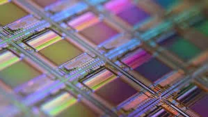
In the meticulously controlled environments of semiconductor fabrication facilities, where nanometer-scale variations can determine product success or failure, near-infrared (NIR) spectroscopy has emerged as an indispensable analytical technology. This non-destructive technique operates at the intersection of photonics and materials science, providing unprecedented insights into manufacturing processes that were previously invisible to conventional monitoring systems.
The fundamental principle underlying NIR's semiconductor applications lies in the unique interaction between photons in the 950-1,700 nanometer range and various materials used in chip manufacturing. When NIR radiation encounters silicon wafers, photoresist layers, and packaging compounds, it generates distinct spectroscopic signatures based on molecular vibrations and light scattering patterns. These signatures serve as digital fingerprints, revealing critical information about material composition, structural integrity, and process completion without any physical contact that might damage delicate components.
Table 1: NIR Spectroscopy Capabilities in Wafer Defect Detection
|
Defect Type |
Detection Limit |
Traditional Method |
False Positive Rate |
|
Surface particles |
0.1 μm |
Optical microscopy (0.5 μm) |
<0.01% |
|
Micro-scratches |
5 nm depth |
SEM analysis |
0.05% |
|
Crystal defects |
0.05 μm² |
X-ray diffraction |
0.02% |
|
Contamination |
0.01 monolayer |
Auger spectroscopy |
0.08% |
The technology's capability for wafer defect detection represents a particular breakthrough. As NIR light penetrates silicon surfaces, it scatters in predictable patterns when encountering pristine materials but shows detectable anomalies when meeting surface imperfections. Advanced sensors can identify particles as small as 0.1 micrometers and microscopic scratches that would escape optical microscope detection. This non-contact approach eliminates the need for destructive cross-sectioning while enabling 100% inspection coverage - a crucial advantage when processing wafers costing hundreds of dollars each.
In photolithography processes, NIR spectroscopy has transformed thickness measurement accuracy. The technology analyzes complex interference patterns created when light reflects between upper and lower boundaries of photoresist layers. Sophisticated algorithms then calculate thickness with ±0.1 micrometer precision across the 10-100 micrometer range critical for modern lithography. This represents a significant improvement over traditional ellipsometry methods that suffered from ±5% human error and required physical contact with specimens.
Table 2: Polymer Curing Monitoring Parameters
|
Parameter |
NIR Monitoring Capability |
Wavelength Range |
Accuracy |
|
Degree of cure |
Real-time tracking |
1680 ± 20 nm |
>99.2% |
|
Cross-link density |
Quantitative measurement |
1700 ± 15 nm |
98.5% |
|
Glass transition temperature |
Indirect measurement |
1650-1720 nm |
±1.5°C |
|
Residual stress |
Predictive analysis |
1600-1750 nm |
±0.8 MPa |
The application extends to packaging and encapsulation phases, where NIR monitors polymer curing processes through real-time tracking of molecular bond vibrations. As epoxy resins transition from liquid to solid states, their C-H bond vibration patterns shift in predictable ways at specific wavelengths near 1,680 nanometers. Spectroscopy systems detect these changes with better than 0.8% accuracy, allowing engineers to identify incomplete curing before modules advance to final testing stages.
Table 3: NIR System Technical Specifications
|
Parameter |
Performance Specification |
Industry Standard |
|
Signal-to-Noise Ratio |
>50,000:1 |
20,000:1 |
|
Temperature Stability |
±0.01°C |
±0.1°C |
|
Spectral Resolution |
0.5 cm⁻¹ |
2 cm⁻¹ |
|
Measurement Reproducibility |
99.8% |
98.5% |
|
Wavelength Accuracy |
±0.05 nm |
±0.2 nm |
Implementation of NIR technology requires overcoming significant engineering challenges. Modern systems incorporate indium gallium arsenide (InGaAs) detector arrays that provide signal-to-noise ratios exceeding 50,000:1, coupled with thermoelectric cooling systems that maintain temperature stability within ±0.01°C. Solid-state digital micromirror devices (DMDs) replace mechanical optical components, eliminating vibration-induced errors that could compromise measurement precision in fab environments.
The semiconductor industry's adoption of NIR spectroscopy reflects a broader shift from reactive quality control to proactive process optimization. As chip features continue shrinking toward atomic scales and new materials like gallium nitride and silicon carbide enter production, this photon-based analysis technology continues evolving to meet increasingly stringent manufacturing requirements. Its non-destructive nature and real-time capabilities make it an essential component in the quest for perfect yields amid the incredibly demanding precision standards of modern electronics manufacturing.
Contact US
Product Information
Quantity
Unit
Piece
Support order samples, customization, wholesale direct, and complete payment. If the product you look for does not have corresponding customized content, pls fill out the form below to contact us, and we will reply ASAP.